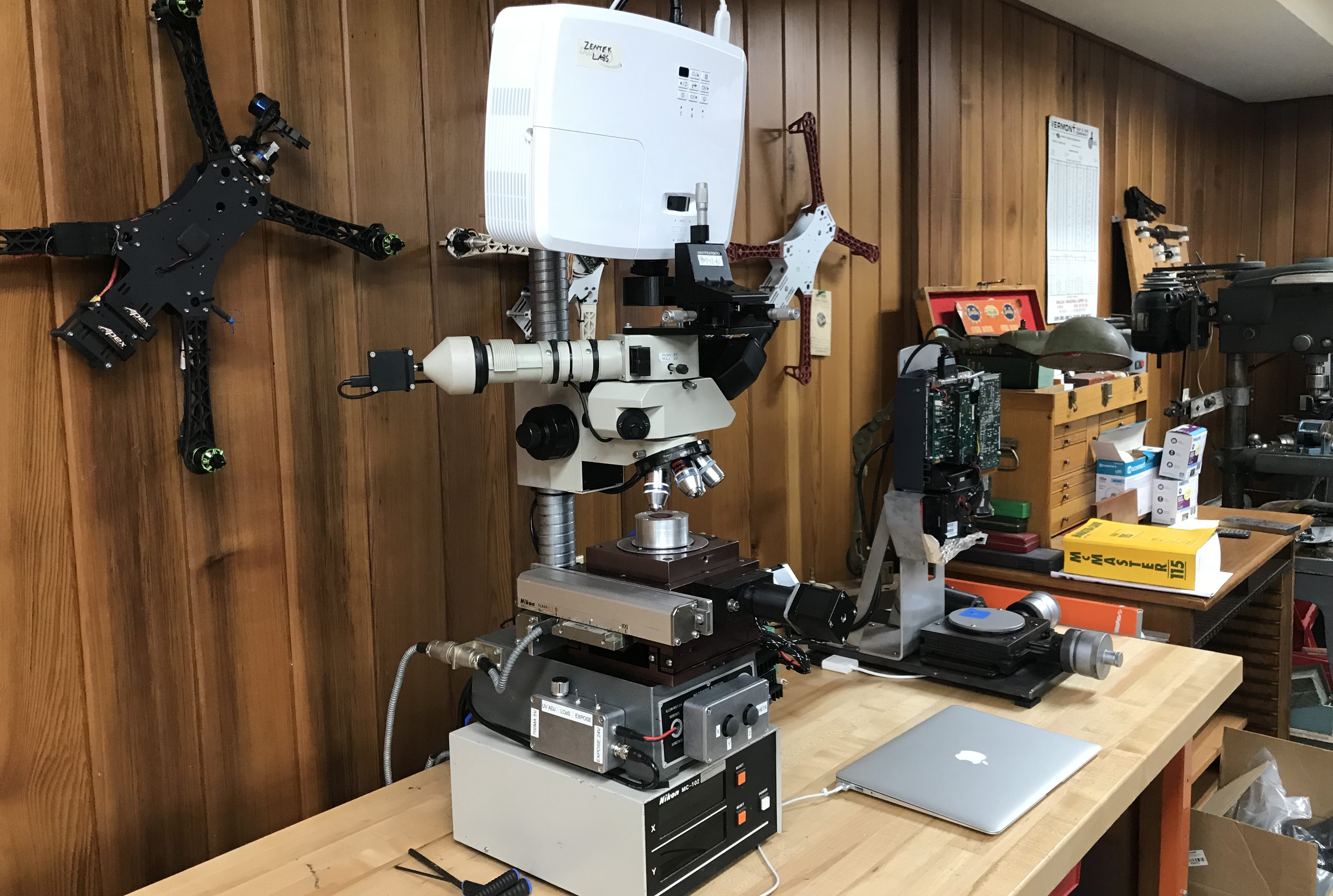
Have a mini-course into maskless photolithography[1][2], and find out how an old DLP projector combined with some advanced optics can yield this: http://sam.zeloof.xyz/wp-content/uploads/2017/02/IMG_2917-e1...
Take a tour in a home fab: https://www.youtube.com/watch?v=TrmqZ0hgAXk
His website and Youtube channel are so richly filled with knowledge that so desperately needs to be in the public domain, instead of being locked in corporate structures.
IEEE has a background piece for those (like me) wondering "who is this guy?"
https://spectrum.ieee.org/semiconductors/devices/the-high-sc...
Impressive.
Impressive to replicate silicon semiconductor process. But wouldn't it be more feasible to develop as good enough process node, flexible, thin film semiconductor devices? Have been observing developments of plastic based transistors, inks, processes like nanoimprint lithography, Cleanroom in a STEM microscope and Chad Mirkin's Tera Print system. Can a small scale nanfab emerge using tech such as Nano-Ops http://nano-ops.net/nanoscale-printing/ ?
I imagine flexible, thin film, large panel based semiconductor SoC. It will not be just a mere microcontroller or IoT node, but a full fleged computing form factor. Think your wall as big plastic computer.
When I read things like this I start to think about the following question: Given no technology at all (i.e. after an apocalypse!), how would one go about creating a computer (as we know them). What sort of knowledge would you need? The science of these things is basically multi decades of trial and error in various disciplines. Imagine a manual that explained how to create everything from scratch!
Geeze, I though you needed a clean room to do this kind of work. I guess, being a hobby, with less concern for effort, loss of product, or cost versus profit, one might summon the will to try, try again, when confronted with botched fabrication runs.
Even with millimeter-scale components, I'd still think dust and debris could be a real problem. Is it just that 12 hour runs are short enough to just accept an imperfect production output, since it's a personal project, or is dust not as big a deal at this scale as I'd imagine?
I was looking for how he managed the clean room or did he not go too small. Found the answer in the IEEE article shared by another commenter (he didn't go below 10 micron tech node).
But now I have a follow up question, if getting a clean room is obviously harder, isn't "clean box" more doable? E.g., if you line up a bunch of tables, and put a long box on top that acts like a poor man's assembly line. The insides of that box are only accessible through gloves that are attached to holes on the sides of the box, and plenty of glass windows to look inside (kinda like the box in movie 'Life'). How cost effective and feasible (i.e., gets the job done) would that be compared to a clean room? maybe you could go sub-micron with it if not sub-100nm.
I predict a future Hacker News submission titled "I turned my garage into an EPA Superfund Site"
This is incredible work. I would have loved to have attempted this when I was in college. The field seemed so inaccessible, and now it makes me happy to see some homebrewer accomplishing things like this.
That's great! Are we anywhere near to making homebrew ICs on silicon at home? Yes, apparently we are! But it seems we are still far away from DIY kits, or even complete prototyping devices (like 3D printers).
If he could get feature size down to 10 microns someone might have a shot at making a microprocessor.
Can the process be streamlined into a single amateur-friendly device/lab? Yes, I mean a chip printer, as a commercial product.
Instead of using all these dangerous chemicals, can you use use an alternative like Ion Beam Etch (IBE) or some sort of plasma etching system (given that a person can build one and has the money for everything like turbopumps and grids)? Or is it mandatory to use something like HF to etch?
Lots of comments on the previous article (before he had a chip to test) as well.
I remember, there is a Swiss guy in HK who is trying to reanimate an abandoned nineties era fab for use by of opensource electronics.
Cheers to this kid's drive and inventiveness, but I won't be at all surprised when his house becomes a Superfund site.
Had a chance to interview Sam last week, he's as bright as you'd assume: https://theamphour.com/390-an-interview-with-sam-zeloof/
There are less dangerous ways to explore "building a CPU from scratch" that hit on the really interesting bits. "Digital Computer Electronics" by Malvino and Brown. You are given logic gates (and, or, nor, nand etc) and build up from there to a working CPU. The articles referenced about HF are terrifying. I am a programmer, but, have worked in a chemistry lap. Its just endless stinky stuff that will kill you in a variety of ways. The logic of how a CPU works is more interesting.
Uoou... now this is really cool, this guy is incredible :)
Lovely, I've always wanted to do something similar.
Bravo!
OK now grow your own SI wafers using repeated Czochralski process based on silicon you made by melting sand.
Awesome. For those considering exploring some of these steps in their own garage -- the chemistry is dangerous, perhaps HF in particular, as it doesn't hurt, it just kills you a few hours later.
Can you do this in a garage? Absolutely, but learn everything you need to know from an ensemble of safety-minded mentors before you strike out on your own.
It's not just about safety for you, proper disposal of these chemicals is essential for the many generations to come. Sometimes it is inexpensive, sometimes it is costly. You need to know how before you start, or it costs a lot more.
(Also, you can get someone else to pay for the hardware, the infrastructure, the material, the resists, the reagents, the safety training, and the waste disposal if you work/volunteer at a university's photolithography facility. They'll probably pay you, too.)